Discovering Graphene
Single-layer graphene was explored theoretically by P. R. Wallace in 1947. It was first unambiguously produced and identified in 2004, by the group of Andre Geim and Konstantin Novoselov, though they credit Hanns-Peter Boehm and his co-workers for the experimental discovery of graphene in 1962. Boehm et al. introduced the term graphene in 1986.
In 1859 Benjamin Collins Brodie became aware of the highly lamellar structure of thermally reduced graphite oxide. The structure of graphite was identified in 1916 by the related method of powder diffraction. It was studied in detail by Kohlschütter and Haenni in 1918, who described the properties of graphite oxide paper. Its structure was determined from single-crystal diffraction in 1924.
The theory of graphene was first explored by P. R. Wallace in 1947 as a starting point for understanding the electronic properties of 3D graphite. The emergent massless Dirac equation was first pointed out by Semenoff, DiVincenzo and Mele. Semenoff emphasized the occurrence in a magnetic field of an electronic Landau level precisely at the Dirac point. This level is responsible for the anomalous integer quantum Hall effect.
The earliest TEM images of few-layer graphite were published by Ruess and Vogt in 1948. Later, single graphene layers were observed directly by electron microscopy Before 2004 intercalated graphite compounds were studied under a transmission electron microscope (TEM). Researchers occasionally observed thin graphitic flakes ("few-layer graphene") and possibly even individual layers. An early, detailed study on few-layer graphite dates to 1962 when Boehm reported producing monolayer flakes of reduced graphene oxide. Starting in the 1970s single layers of graphite were grown epitaxially on top of other materials. This "epitaxial graphene" consists of a single-atom-thick hexagonal lattice of sp2-bonded carbon atoms, as in free-standing graphene. However, significant charge transfers from the substrate to the epitaxial graphene, and in some cases, the d-orbitals of the substrate atoms hybridize with the π orbitals of graphene, which significantly alters the electronic structure of epitaxial graphene.
Single layers of graphite were observed by TEM within bulk materials, in particular inside soot obtained by chemical exfoliation. Efforts to make thin films of graphite by mechanical exfoliation started in 1990, but nothing thinner than 50 to 100 layers was produced before 2004.
Graphene, a two-dimensional form of crystalline carbon, either a single layer of carbon atoms forming a honeycomb (hexagonal) lattice or several coupled layers of this honeycomb structure. The word graphene, when used without specifying the form (e.g., bilayer graphene, multilayer graphene), usually refers to single-layer graphene. Graphene is a parent form of all graphitic structures of carbon: graphite, which is a three-dimensional crystal consisting of relatively weakly coupled graphene layers; nanotubes, which may be represented as scrolls of graphene; and buckyballs, spherical molecules made from graphene with some hexagonal rings replaced by pentagonal rings.


The basic electronic structure of graphene and, as a consequence, its electric properties are very peculiar. By applying a gate voltage or using chemical doping by adsorbed atoms and molecules, one can create either electron or hole (a region where an electron is missing that acts as a positive electric charge) conductivity in graphene that is similar to the conductivity created in semiconductors. However, in most semiconductors there are certain energy levels where electrons and holes do not have allowed quantum states, and, because electrons and holes cannot occupy these levels, for certain gate voltages and types of chemical doping, the semiconductor acts as an insulator. Graphene, on the other hand, does not have an insulator state, and conductivity remains finite at any doping, including zero doping. Existence of this minimal conductivity for the undoped case is a striking difference between graphene and conventional semiconductors. Electron and hole states in graphene relevant for charge-carrier transport are similar to the states of ultra-relativistic quantum particles—that is, quantum particles moving at the speed of light (the ultimate velocity in nature, according to the theory of relativity).
The honeycomb lattice of graphene actually consists of two sublattices, designated A and B, such that each atom in sublattice A is surrounded by three atoms of sublattice B and vice versa. This simple geometrical arrangement leads to the appearance that the electrons and holes in graphene have an unusual degree of internal freedom, usually called pseudospin. In fact, making the analogy more complete, pseudospin mimics the spin, or internal angular momentum, of subatomic particles. Within this analogy, electrons and holes in graphene play the same role as particles and antiparticles (e.g., electrons and positrons) in quantum electrodynamics. At the same time, however, the velocity of the electrons and holes is only about 1/300 the speed of light. This makes graphene a test bed for high-energy physics: some quantum relativistic effects that are hardly reachable in experiments with subatomic particles using particle accelerators have clear analogs in the physics of electrons and holes in graphene, which can be measured and studied more easily because of their lower velocity. An example is the Klein paradox, in which ultra-relativistic quantum particles, contrary to intuition, penetrate easily through very high and broad energy barriers. Thus, graphene provides a bridge between materials science and some areas of fundamental physics, such as relativistic quantum mechanics.
There is another reason why graphene is of special interest to fundamental science: it is the first and simplest example of a two-dimensional crystal—that is, a solid material that contains just a single layer of atoms arranged in an ordered pattern. Two-dimensional systems (surfaces, membranes, and interfaces) are of huge interest not only for physics and chemistry but also for biology and other natural sciences. (For example, cell membranes, which are crucially important for life, are essentially made up of sheets of lipid molecules with embedded proteins.) In many respects, two-dimensional systems are fundamentally different from three-dimensional systems. In particular, due to very strong thermal fluctuations of atomic positions that remain correlated at large distances, long-range crystalline order cannot exist in two dimensions. Instead, only short-range order exists, and it does so only on some finite scale of characteristic length—a caveat that should be noted when graphene is called a two-dimensional “crystal.” For this reason, two-dimensional systems are inherently “flexural,” manifesting strong bending fluctuations, so that they cannot be flat and are always rippled or corrugated. Graphene, because of its relative simplicity, can be considered as a model system for studying two-dimensional physics and chemistry in general. Other two-dimensional crystals besides graphene can be derived by exfoliation from other multilayer crystals (e.g., hexagonal boron nitride, molybdenum disulfide, or tungsten disulfide) or by chemical modification of graphene (e.g., graphane, hydrogenated graphene, or fluorinated graphene).
Modern electronics (e.g., integrated circuits in computer chips) are basically two-dimensional in that they use mainly the surface of semiconducting materials. Therefore, graphene and other two-dimensional materials are considered very promising for many such applications. Using graphene, for example, it should be possible to make transistors and other electronic devices that are much thinner than devices made of traditional materials. Many other applications have been proposed. For example, graphene, being electrically conducting, transparent, strong, and flexible, may be a prospective material for use in touch screens. Graphene also has very high thermal conductivity and, therefore, could be used to remove heat from electronic circuits. Being very strong mechanically, it could be used as a scaffold for studying biological molecules and materials.

Discovery
Initial attempts to make atomically thin graphitic films employed exfoliation techniques similar to the drawing method. Multilayer samples down to 10 nm in thickness were obtained. Earlier researchers tried to isolate graphene starting with intercalated compounds, producing very thin graphitic fragments (possibly monolayers). Neither of the earlier observations was sufficient to launch the "graphene gold rush" that awaited macroscopic samples of extracted atomic planes.
One of the first patents pertaining to the production of graphene was filed in October 2002 and granted in 2006. It detailed one of the first large scale graphene production processes. Two years later, in 2004 Geim and Novoselov extracted single-atom-thick crystallites from bulk graphite. They pulled graphene layers from graphite and transferred them onto thin silicon dioxide (SiO2) on a silicon wafer in a process called either micromechanical cleavage or the Scotch tape technique. The SiO2 electrically isolated the graphene and weakly interacted with it, providing nearly charge-neutral graphene layers. The silicon beneath the SiO2 could be used as a "back gate" electrode to vary the charge density in the graphene over a wide range. US patent, filed in 2002, describes how to process expanded graphite to achieve a graphite thickness of one hundred-thousandth of an inch (0.25 nm). The key to success was high-throughput visual recognition of graphene on a properly chosen substrate that provides a small but noticeable optical contrast.

The cleavage technique led directly to the first observation of the anomalous quantum Hall effect in graphene, which provided direct evidence of graphene's theoretically predicted Berry's phase of massless Dirac fermions. The effect was reported by Geim's group and by Kim and Zhang, whose papers appeared in Nature in 2005. Before these experiments other researchers had looked for the quantum Hall effect and Dirac fermions in bulk graphite.
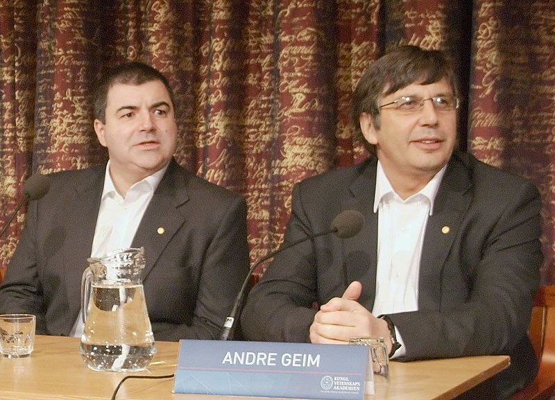
Geim and Novoselov received awards for their pioneering research on graphene, notably the 2010 Nobel Prize in Physics.
In the decades that followed, it remained difficult to say which applications would prove to be the most popular. Progress depends not only on the basic science but also on the development of new ways to produce graphene on an industrial scale. (Obtaining graphene by exfoliation is too expensive for mass production.) Methods proposed include the formation of graphene layers by burning silicon carbide or by chemical vapour deposition of carbon on the surface of some metals such as copper or nickel. These methods would allow the production of samples of graphene that were macroscopically large in two dimensions (up to tens of centimetres) but still atomically thin.
null

REFERENCES
The University of Manchester. Available in: https://www.graphene.manchester.ac.uk/learn/discovery-of-graphene/. Access in: 28/10/2018.
Physics Today. Available in: https://physicstoday.scitation.org/do/10.1063/PT.4.0866/full/. Access in: 28/10/2018.
Encyclopædia Britannica. Available in: https://www.britannica.com/science/graphene. Access in: 28/10/2018.
Wikipedia. Available in: https://en.wikipedia.org/wiki/History_of_graphene. Access in: 28/10/2018.


0 comments
Sign in or create a free account